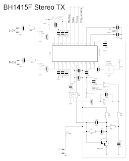
.
OscillatorThe
RF-oscillator is available at pins 3-7. The oscillator operates as a symmetrical Colpitts circuit. The oscillator chip ground, pin 5, should be connected to ground at the
resonance circuit shielding point. An external oscillator can be injected inductively or capacitively via pins 3 and 7.
The layout of the
TV RF Modulator PCB should be such as to provide a minimum shielding attenuation between the
oscillator pins 3-7 and
modulator output pins 15-17 of approximately 80 dB.
For optimal residual
carrier suppression, the symmetrical mixer outputs at pins 15, 17 should be connected to a matched balanced-to-unbalanced
broadband transformer, e.g. a Guanella transformer with good phase precision at 0o and 180o. The
transmission loss should be less than 3 dB. In addition, an
LC-low pass filter combination is required at the output. The cut-off frequency of the
low pass filter combination must exceed the maximum operating frequency.
VideoThe video signal of the
tv rf modulator with the negative synchronous level is capacitively connected to pin 12. The internal clamping circuit is referenced to the synchronizing level. Should the video signal change by 6 dB, this change will be compensated by the
resonance circuit which is set by the peak white value. At pin 13, the current pulses of the peak white detector are filtered through the capacitor which also determines the control time constant. The
RF carrier switches from
negative to positive video modulation, when pin 14 is connected to ground. By varying the value of resistance R at pin 14 between ¥ ... 0 W the modulation depth can be increased from 70% to 100% when the modulation is negative and decreased from 100% to 70% when the modulation is positive.
AudioVia pin 1, the audio signal is capacitively coupled to the AF-input for the
FM-modulation of the
oscillator. A parallel resonance circuit is connected to the audio carrier oscillator at pins 19, 20. The unloaded Q of the resonant circuit must be Q = 25 and the parallel resistor RT = 8.2 kW to ensure a video to audio carrier ratio of 12.5 dB. At the same time, the capacitative and/or inductive reactance for the resonance frequency should have a value of XC » XL » 800 W.
Via pin 18, the audio signal is capacitively coupled to the AF-input for the
AM-modulation of the
oscillator. This signal is forwarded to a mixer which is influenced by the AM modulation input of pin 18. The
video to audio carrier ratio can be changed by connecting an external voltage to pin 18, which deviates from the internal reference voltage. Through an additional external dc voltage at pin 18, the set AM-modulation index can be changed by overriding the internally
adjusted control voltage for a fixed
AM-modulation index.
At the output of the above described mixer the FM and/or
AM modulated audio signal is
added to the
video signal and mixed with the oscillator signal in the RF-mixer.
SourceThe internal reference voltage is available at pin 2 and has to be capacitively blocked there. (For the details, please download
datasheet)
See more:
TV Transmitter -
VHF UHF TV Modulator -
Transistor FM Transmitter 


